For a long while I have been looking for a nice PCB package as I want on occasion to make the odd board or two.
I have tried a few. KiCad so far is the only package that has not frustrated me beyond getting further than a day or so of messing around.
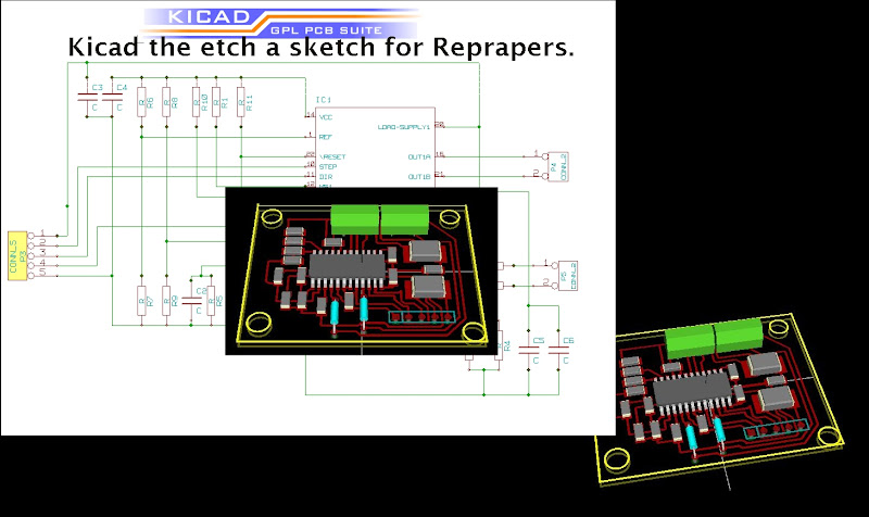
It gave me this nice result for a single sided micro stepper design that I can etch at home.
The only struggle I had and still have was creating a thermal pad so far I can create it.
I can see it but if I try to Print it the thermal pads vanish from my board design..
So I will stick some tape down where my thermal pads should be before I etch the board.
So if any of you know how to do thermal pads that will print for etching in Ki-Cad please please let me know.
Note you see them on your design absolutely great!! Try any combination of printing or plottingng saving to file they Vanish one of the Two bugs I found the other is in the electrical test thing in the cct / Schmatic drawing program I always have an error showing. Seems that its a random error as its different any time you try to change the part of-the error that is not there as it moves some where else.
Special thanks must go to AK47, Nophead and Grael in the Forums who all suggested Ki Cad very pleased !
I will be etching this board shortly.
Next job I now have is to take 4 CA-42 Nokia leads and turn them into 4 Serial leads for my controller boards thus saving well over $80 - $100 as I believe a serial lead is $20 US.
So just one serial cable for me would be $20 + Air freight cost + £8 import handling + %17.5 VAT
10 comments:
My extruder controller has a thermal pad with vias in it and it definitely comes out on the PCB. I will have a look this evening to remind myself how I did it.
I think it is just an extra pad in the library symbol and I had to add the vias at the board level, which was a pain.
Aha did you have th same problem then ?
Where you set the perimiter of the Thermal pad by drawing on your PCB layout it then filling it so you can see it on your board layout screen.
But when you print it the pad is not printed..?
Will add a picture crom Kicad.. to this post..
I am looking at single-sided stepper driver boards I can make at home. I've re-designed the MakerBot Stepper driver to print single-sided - I'm planning to etch it and give it a go soon.
Would you mind posting the board files so I can have a look? I'm quite interested
:-)
Renoir (Dave Reynolds)
I think I just added an extra pin to the chip called PAD. You can see it in the schematic. I then added it to the footprint as a big pad in the middle. That is easy.
Adding the thermal vias is easy but time consuming and because it is at the board level you have to do it each time the chip is used.
The tricky part is the paste mask contraction. Thermal pads need a much bigger contraction and because they are big you need to split them into four quarters. Again I had to do it at the PCB level because the footprints don't have a paste mask layer.
A similar problem with fiducials which need custom solder mask clearance.
Renoir,
Oh yes as soon as I have tested it and got it working.
Which won't be long once I have the boards etched.. I hope.
I do have several chips I'm trying out to get the best performance / cost for the final design.
I found it was quicker to route track by hand as the Auto router is kind of.. erm Stupid.. Maybe Its OK on double sided thou.
Nophead Aha.. Thank you.. Oh I have managed to get the thermal pad to work once. since my reply don't know why it worked. No extra pin..
So I do now know instead of just edge hatching and highlighting the area it fills the area in solid. Wen it works correctly. Just cant see what I did different and can't re-create it..
So going to try the extra Pin called Pad.
The chip I'm using in this case has not got a Pad it just needs copper under it.
Not got any Vias as its Single sided board used upside down.
I still think it should work without a pad though. For example just to make GND planes on RF/HF type boards or maximising copper for high current GND returns.
Or just for improving etching efficiency.
Despite this complaint and its some times tedious nature it is better than any other Free PCB design package!!!..
Solved.. Thank You Nophead!!!
The clue was Pad when it worked I had included the whole of one of the IC pads if you dont use the pad outline i.e only part of it / it fails.
Sucess I bet its in the Destructions some where and I missed it!
Else
The Destructions need that bit added.!!
If its only copper underneath without a connection the you just need a copper fill on the right layer.
I tried that, Its still got some strangeness / there is a Nack to getting the fill to work.. Correctly on anything not marked GND.
So I found its just a whole lot better lableing the NET with a GND symbol then as long as you included a pad that is in the GND NET it works fine.
Its a pity I wanted more copper under the chip, that would need to be isolated but couldn get the Exclude Pad option to work only Thermal seems to work.
I had most fills on GND but some on 12V and it worked fine. The only strangeness I found was in the 3D view. There is an option to fill with tracks or polygons and polygons only show an outline in the the 3D view.
Why do you want electrically and thermally isolated copper under a chip?
The chip requires lots of copper but i have cct tracks under the chip as well so inbetween tracks i wanted extra copper its heatsinking.
Post a Comment